Shift register (output)
The 74HC595: an 8-bit serial-in/serial or parallel-out shift register with a storage register and 3-state outputs.
If higher load is required there is also the TPIC6C595 (e.g., for driving LEDs), or it should be paired with for example ULN2803 or similar. For multiple inputs see the 74HC165.
The basic usage is to serially transfer a byte from a microcontroller to the IC. When latched the byte will then in parallel be available on output pins QA-QH (Q0-Q7).
Hereby we can increase the number of available pins from 3 (data pin, clock, latch pins) to 8. Since the IC can be daisy-chained we can even increase the number of output pins.
Wiring is simple:
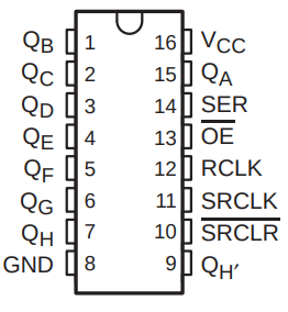
- Pin 16 (VCC): Voltage 5V
- Pin 14 (SER): Data input
- Pin 13 (OE): GND (Output-enable, active low)
- Pin 12 (STCLK): Store clock/latch pin
- Pin 11 (SHCLK): Shift clock pin
- Pin 10 (SRCLR): 5V (master reset)
- Pin 15,1,…7: Output pims
- Pin 8 (GND): GND
When the SHCLK goes high register is shifted and first bit will be set to value of SER. When STCLK (Latch) is pulled high the output pins QA-QH will be updated.
A simple AVR-C example (here for attiny13)
#include <util/delay.h>
#include <avr/io.h>

#define DATA_PORT		PORTB
#define DATA_DDR		DDRB

#define DATA    PB0      // Data pin (DS) pin location
#define CLOCK   PB2      // Shift Clock (SH_CP) pin location
#define LATCH   PB1      // Store Clock (ST_CP) pin location

#define HC595DataHigh() (DATA_PORT|=(1<<DATA))
#define HC595DataLow()  (DATA_PORT&=(~(1<<DATA)))
void HC595Pulse() { // Pulse the Shift Clock
  DATA_PORT|=(1<<CLOCK);    // HIGH
  DATA_PORT&=(~(1<<CLOCK)); // LOW
}
void HC595Latch() { // Pulse the Store Clock
  DATA_PORT|=(1<<LATCH);    // HIGH
  _delay_ms(1);
  DATA_PORT&=(~(1<<LATCH)); // LOW
  _delay_ms(1);
}

void HC595Write(uint8_t data) {
  //Send each 8 bits serially
  //Order is MSB first
  for(uint8_t i=0;i<8;i++) {
    //Output the data on DS line according to the Value of MSB
    if(data & 0b10000000) {
      HC595DataHigh(); //MSB is 1 so output high
    } else {
      HC595DataLow(); //MSB is 0 so output high
    }
    HC595Pulse();  //Pulse the Clock line
    data=data<<1;  //Now bring next bit at MSB position
  }
  //Now all 8 bits have been transferred to shift register
  //Move them to output latch at one
  HC595Latch();
}
void HC595Init() { // Initialize HC595
  // Make the Data(DS), Shift clock (SH_CP), Store Clock (ST_CP) lines output
  DATA_DDR|=((1<<DATA)|(1<<CLOCK)|(1<<LATCH));
}

uint8_t led_pattern[8]={0b10000001,
		      0b11000011,
		      0b11100111,
		      0b11111111,
		      0b01111110,
		      0b00111100,
		      0b00011000,
		      0b00000000};

int main(void) {
  HC595Init();
  HC595Write(0b00000000);
  _delay_ms(100);

  while (1) {
    for (unsigned i=0; i<8; i++) {
      HC595Write(led_pattern[8-i]);
      _delay_ms(100);
    }
    for (unsigned i=0; i<8; i++) {
    HC595Write(led_pattern[i]);
    _delay_ms(100);
    }
  }
}
Arduino example with
- Pin 14 (SER) attached to D2
- Pin 12 (STCLK) attached to D3
- Pin 11 (SHCLK) attached to D4
Here two shift registers are daisy-chained by wiring pin 9 (QH’) of the first register to the SER/DATA pin of the second register. All other pins should be wired identically.
// Mux (output:74HC495, input:74HC165)
// Author: Klaus Holst, 2019

const unsigned dataPin = 2;  // Data pin (DS/SER) of 74HC595
const unsigned latchPin = 3; // Store clock (ST_CP/RCLK)   of 74HC595
const unsigned clockPin = 4; // Shift-clock (SH_CP/SRCLK) of 74HC595

void setup() {
  // Serial.begin(115200);
  // Serial.println("Log start:\n");
  pinMode(LED_BUILTIN,  OUTPUT);
  pinMode(latchPin, OUTPUT);
  pinMode(clockPin, OUTPUT);
  pinMode(dataPin, OUTPUT);
}

// Send 1 to the first shift register, and numbers from 0 to 64 to the second.
void send() {
  for (unsigned i=0; i<64; i++) {
    digitalWrite(latchPin, LOW); // ground latchPin and hold low for as long as you are transmitting
    // shiftOut(dataPin, clockPin, bitOrder, value)
    // bitOrder: MSBFIRST or LSBFIRST. (Most Significant Bit First, or, Least Significant Bit First).
    // value: type byte
    shiftOut(dataPin, clockPin, MSBFIRST, i); // Input B, 8bits
    shiftOut(dataPin, clockPin, MSBFIRST, 1); // Input A, 8bits
    delay(100);
    digitalWrite(latchPin, HIGH); //return the latch pin high to signal chip that it no longer needs to listen for information
  }
}

void loop() {
  send();
}