Shift register circuit board
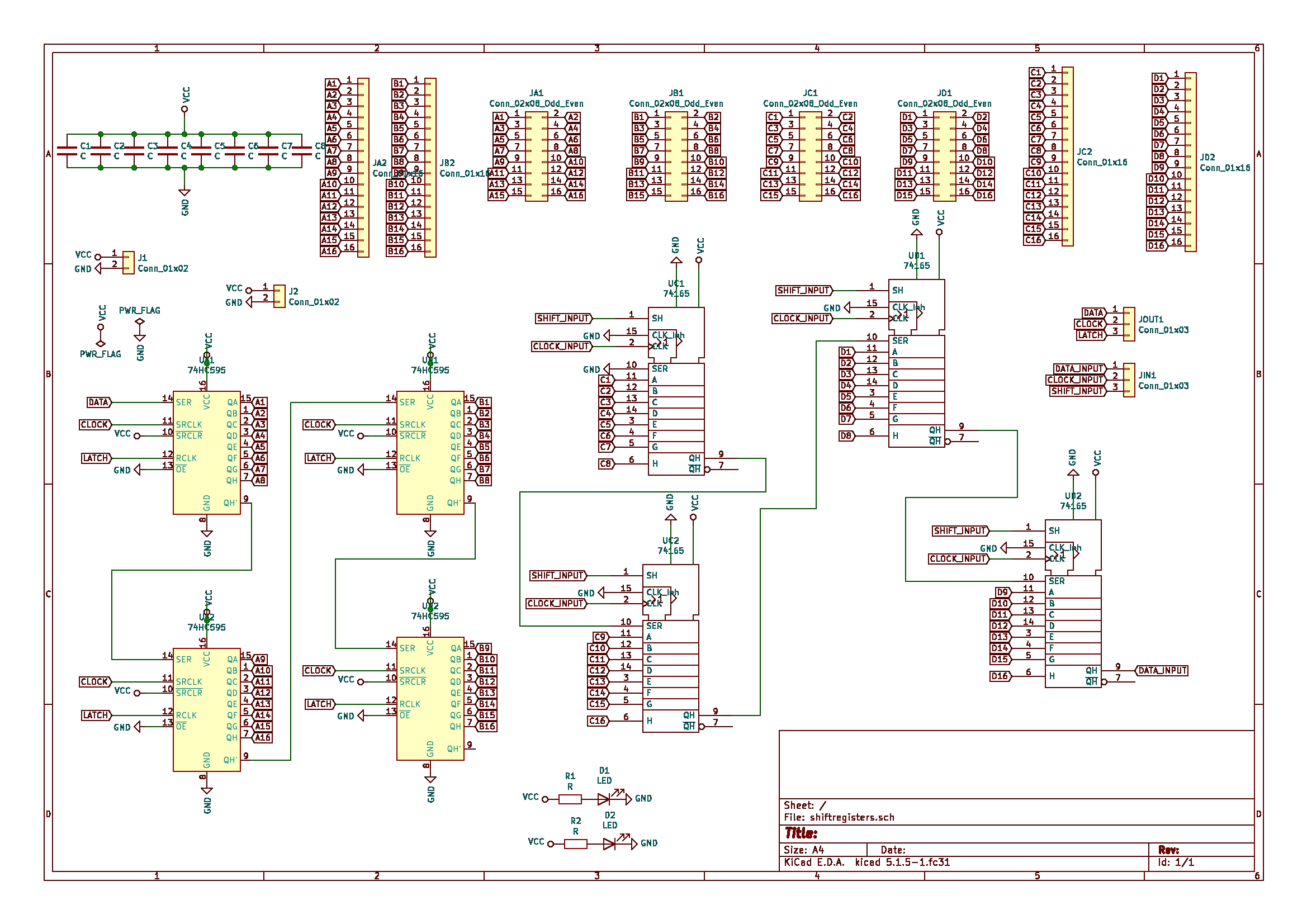
The
74HC165 and
74HC495 are useful integrated circuits for dealing
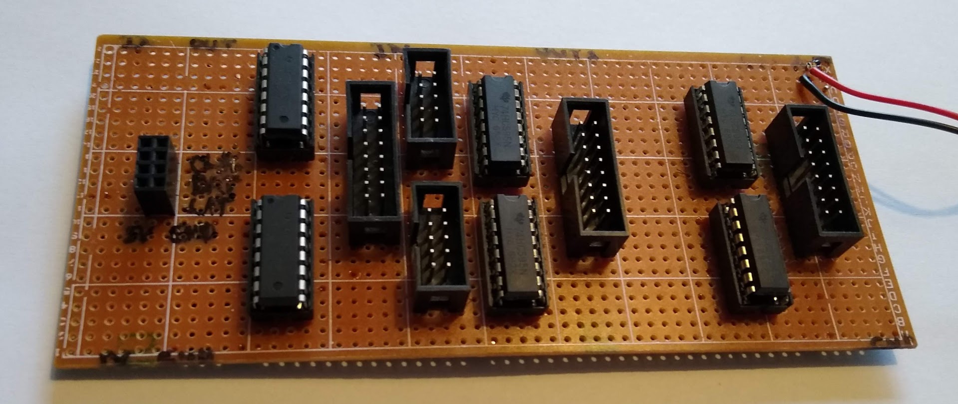
with multiple digital inputs and outputs. In a recent project, I used the following prototype based on a variant of the above simple circuit schema:
The four 74HC495 ICs gives access to 2 x 16 bits accessible through IDC connectors controllable using just three pins on the microcontroller (DATA, CLOCK, LATCH). Similarly, two 74HC165 ICs gives access to 16 input bits through another IDC connector.
<!–more–>
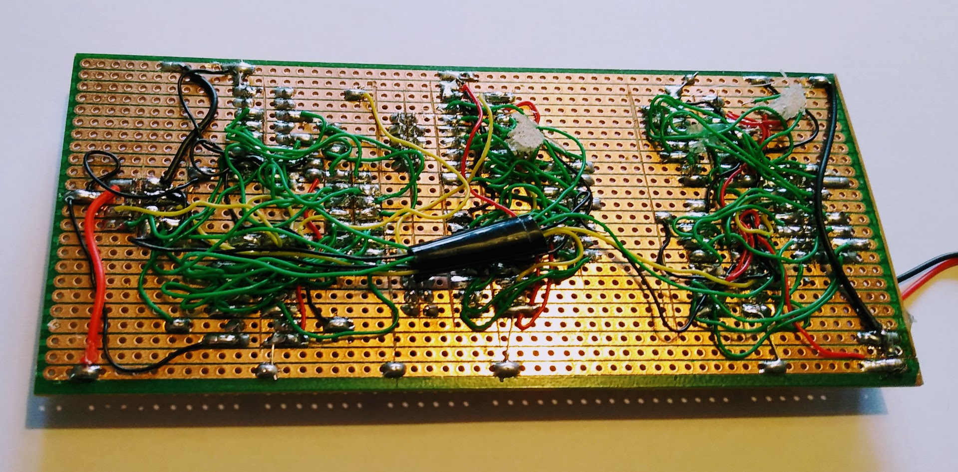
While doing the job, the wiring was so embarrassing that I decided to finally move to a PCB design (using
KiCad) based on surface-mounted components.
The Gerber files are available
here and this is what the final assembled circuit looks like (2 x 16 bit input and 2 x 16 bit output, dimensions: 51mm x 70mm):
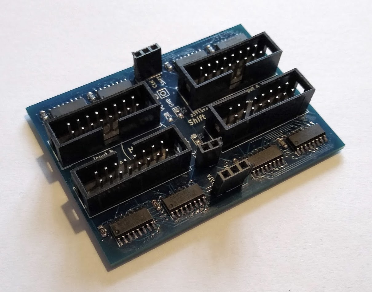
Component list:
- 4 x 74HC595 SOIC-16 3.9mmx9.9mm P1.27mm (UA1,UA2,UB1,UB2)
- 4 x 74HC165 SOIC-16 3.9mmx9.9mm P1.27mm (UC1,UC2,UD1,UD2)
- 8 x 0.1uF Ceramic Capacitor SMD 0805 (C1-C8)
- 4 x IDC 16 pin connectors 2x8 P2.54mm (JA1, JB1, JC1, JD1)
- Optional: 2 x 330R resistor SMD 0805
- Optional: 2 x LED SMD 0805
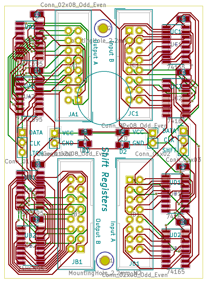
The output (74HC595) is controlled from the left side inputs which are marked on the PBC as: DATA, CLK, LTCH. Similarly, the input (74HC165) is controlled from the right side inputs: DATA, CLK, SHFT. 5V DC must be supplied to either of the two DC-inputs marked on the PBC.
The following Arduino C++ code illustrates the usage of the board with pins 12,11,10 connected to DATA, CLK, LTCH.
  const uint8_t dataPin  = 12;
  const uint8_t clockPin = 11;
  const uint8_t latchPin = 10;

  void setup() {
    pinMode(dataPin, OUTPUT);
    pinMode(clockPin, OUTPUT);
    pinMode(latchPin, OUTPUT);
  }

  void send(int myword, unsigned wait=0) {
    digitalWrite(latchPin, LOW); // ground latchPin and hold low for as long as you are transmitting
    shiftOut(dataPin, clockPin, MSBFIRST, highByte(myword)); // Input B, 8bits
    shiftOut(dataPin, clockPin, MSBFIRST, lowByte(myword));  // Input A, 8bits
    digitalWrite(latchPin, HIGH); // return the latch pin high to signal chip that it no longer needs to listen for information
    if (wait>0) delay(wait);
  }

  const unsigned wait = 20;

  void loop() {
    unsigned val = 1;
    for (unsigned i=0; i<15; i++) {
      send(val, wait);
      val = val<<1;
    }
    for (unsigned i=0; i<15; i++) {
      send(val, wait);
      val = val>>1;
    }
  }
This produces a
Knight Rider effect on the output JA1 as illustrated in the following video:
16 bit gate
The Gerber files for the 16 bit gate used in the above video is available here. It is quite useful for testing purposes (with the LED interface) and for easy wiring to the IDC interface.
Component list:
- 2 x ULN2803a (SOIC-18W, 7.5x11.6mm, P1.27mm)
- 4 x IDC 16 pin connectors (2x8 P2.54mm)
- 16 x LED SMD 0805
- 16 x 330R Resistors SMD 0805
A pair of decoupling capacitors should probably be added to this design at some point…
The ribbon cable assembly is pretty straightforward as shown in this short video: